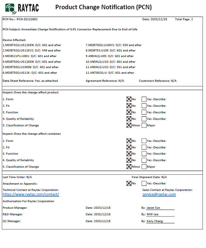
There are no changes on Form, Fit, Function, and Quality of Reliability. Only change in u.FL Connector Appearance. All existing certifications and technical documentations remain valid.
We kindly invite our customers, distributors, and partners to update your records accordingly. For any questions or support regarding this update, feel free to reach out via: sales@raytac.com.
Raytac’s AN54LQ & AN54LV modules, powered by Nordic Semiconductor’s nRF54L family SoCs, come in multiple form factors and antenna options, ensuring your seamless integration into compact, RF-sensitive, or performance-driven designs.
Whether you need a: ☑ Chip antenna; ☑ PCB antenna; ☑ u.FL connector; ☑ Antenna Pin,
Or you want Small, Smaller, or Smallest, we always have a solution that fits best! *All products are pre-certified with FCC, IC, CE, UKCA, Telec, KC, SRRC, NCC, RCM, WPC.
17800 Castleton Street, Suite 238, City of Industry, CA 91748, USA Phone: 626.328.3827 Our new location strengthens our operational capabilities in the United States, enabling faster logistics, enhanced customer support, and expanded service coverage. We look forward to continuing to serve our partners and customers from our new facility.
Raytac has advanced the dev kit of bundle offer – WIFI+BLE: AN7002Q-DB-5340-M with an on-board flash memory(MX25R64) to create easy evaluation for Wi-Fi project developments.
[January 2026 Update] In this article, we will talk about: Project WITH External Flash MX25R64(8MB) applied - Connecting through SPI between nRF5340 module: MDBT53-1M(BLE) & nRF7002 module: AN7002Q(WIFI) - Connecting through QSPI (XIP) between MDBT53-1M and external memory MX25R64
Table of Content———————————————————————————————
Hardware Set Up A. Project WITHOUT External Flash MX25R64 needed B. Project WITH External Flash MX25R64 needed
Software Resources & Preparations
Firmware Build & Compile A. Project WITHOUT External Flash MX25R64 needed B. Project WITH External Flash MX25R64 needed
Note: Pease make sure to have both “Nordic nRF5340-DK” and “AN7002Q-DB-5340-M”connected and running during the WIFI+BLE (nRF7002+nRF5340) project development.
Hardware Network: IDC Ribbon Wire(J-Link Cable): Connect nRF5340-DK to AN7002Q-DB-5340-M USB Wire –Type C USB: Power supply to AN7002Q-DB-5340-M through USB TYPE-C USB Wire-Micro USB: Power supply to nRF5340-DK through Micro USB
Schematic diagram of AN7002Q-DB-5340-M can be referenced for design as follows.
The circuit of SW1(p1.08)/SW2(p1.09)/LED1(p1.06) on AN7002Q-DB-5340-M is NOT COMPATIBLE to Nordic WI-FI Control Pin of swctrl1(p1.08)/host_irq(p1.09)/grant(p1.06). In this case, if you’re working with external flash MX25R64 for the WIFI project, Please avoid pin SW1/SW2/LED1 usage while LED2(p1.07) remains available as normal usage. For the PCB design of end product/end device(mounted with AN7002Q & MDBT53 modules), the switch & LED should be configured to be SW1(p0.23)/SW2(p0.24)/LED1(p0.28).